CNC Machining for Semiconductor Equipment: Ultra-Precision Requirements
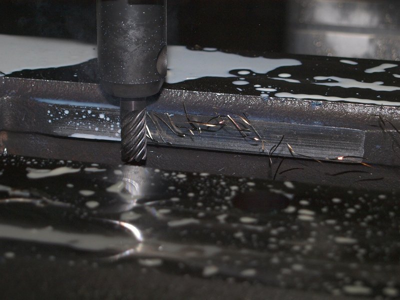
Introduction: The Critical Role of Precision Machining in Semiconductor Manufacturing
The semiconductor industry represents the pinnacle of modern precision engineering. As transistor geometries shrink below 3 nanometers and wafer diameters expand to 300 mm, the mechanical components inside semiconductor fabrication equipment must achieve levels of accuracy that few other industries require. According to SEMI (Semiconductor Equipment and Materials International), global semiconductor manufacturing equipment sales reached approximately US$165.9 billion in 2026, reflecting a 23.2% year-over-year increase driven by AI accelerator chips, 5G infrastructure, and high-performance computing.
For manufacturers of semiconductor equipment, the quality of CNC-machined parts directly determines tool performance, wafer yield, and production uptime. This article explores the ultra-precision requirements, materials, manufacturing processes, and quality standards that define CNC machining for semiconductor equipment applications.
Industry Insight: An advanced EUV lithography machine consists of over 250,000 parts, of which approximately 90% are CNC-machined, and more than 40% are ultra-high precision components.
What Is Ultra-Precision CNC Machining for Semiconductor Equipment?
Ultra-precision CNC machining for semiconductor equipment refers to the computer-controlled material removal process used to fabricate components for wafer fabrication equipment (WFE), metrology tools, and packaging systems. Unlike conventional machining, semiconductor-grade CNC machining demands simultaneous control of dimensional accuracy, surface integrity, contamination levels, and material traceability.
The key distinction lies in the combination of requirements. A single component may need to meet dimensional tolerances of ±0.005 mm, flatness below 0.01 mm, surface finish Ra 0.4 μm, zero burrs, particle-controlled cleanliness, and full material certification—all at once. This makes semiconductor equipment machining one of the most technically challenging areas of precision manufacturing.
Dimensional Tolerance
±0.005 mm (standard)
±0.002 mm (precision)
±0.001 mm (ultra-precision)
Flatness Requirement
≤ 0.01 mm (standard)
≤ 0.005 mm (critical)
Often more critical than linear dims
Surface Finish
Ra 0.4–0.8 μm (standard)
Ra 0.1–0.2 μm (precision)
Ra 0.05 μm (mirror finish)
Cleanliness Class
Class 100 / ISO 5
Ultra-high vacuum compatible
Zero particle generation
Key Precision Requirements in Semiconductor Equipment Components
Sub-Micron Dimensional Tolerances
While conventional machining may allow tolerances of ±0.05 mm, semiconductor parts frequently require ±0.005 mm or tighter. For the most demanding applications—such as wafer positioning systems, optical alignment fixtures, and precision vacuum chucks—tolerances of ±2 μm are considered moderate, and ±1 μm is often necessary for next-generation equipment.
Surface Finish as a Functional Requirement
In semiconductor equipment, surface finish is not merely cosmetic—it directly affects contamination risk and process performance. A smooth surface retains fewer particles, improves cleaning efficiency, supports vacuum sealing, reduces wear, and improves process consistency. Wetted surfaces require Ra ≤ 0.4 μm, while wafer-contact surfaces demand Ra ≤ 0.1 μm or better.
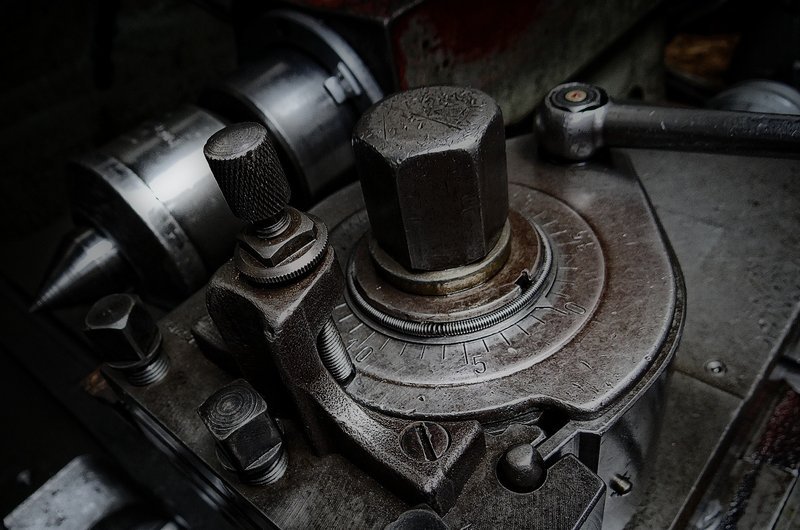
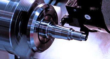
Precision-machined semiconductor chamber components require ultra-smooth surfaces and zero-contamination finishes.
Flatness and Geometric Controls
Flatness frequently matters more than dimensional accuracy in semiconductor components. A vacuum chamber cover with acceptable dimensions but inadequate flatness can compromise vacuum integrity, leading to process failures. Typical flatness requirements for critical sealing surfaces are ≤ 0.01 mm, with some components requiring ≤ 0.005 mm over spans of 200 mm or more.
Contamination Prevention and Cleanroom Standards
Dimensional compliance alone is insufficient. Semiconductor parts must be manufactured in cleanroom-compatible environments to prevent particle, ionic, hydrocarbon, metallic, and airborne molecular contamination. This requires multi-stage ultrasonic cleaning with deionized water, vacuum bake-out cycles, and Class 100 cleanroom packaging. Outgassing rates must typically meet TML ≤ 1% and CVCM ≤ 0.1% per ASTM E595.
Materials Used in Semiconductor Equipment CNC Machining
Material selection for semiconductor equipment components must balance chemical inertness, thermal stability, dimensional precision, and vacuum compatibility.
| Material | Key Properties | Common Applications |
|---|---|---|
| Aluminum 6061-T6 / 7075-T6 | Lightweight, high machinability, low outgassing | Chamber housings, wafer handlers, base plates |
| Stainless Steel 316L / 304 | Corrosion resistant, vacuum-compatible, electropolishable | Gas distribution plates, vacuum hardware |
| Titanium Ti-6Al-4V | High strength-to-weight, corrosion resistant | Vacuum flanges, RF electrodes |
| PEEK / Vespel | Low outgassing, chemical resistant, electrical insulation | End effectors, wafer grippers, insulators |
| Alumina / Silicon Carbide | Dielectric, wear-resistant, heat-tolerant | Plasma chambers, electrostatic chucks |
Core Machining Processes for Semiconductor Components
Ultra-Precision Milling
Multi-axis CNC milling is the most versatile process for semiconductor components. High-speed spindles (up to 40,000 RPM), extremely sharp cutting tools, and small depths of cut minimize cutting force while achieving mirror-like surface finishes. Temperature-controlled environments are essential to prevent thermal expansion errors.
Precision Turning and Grinding
Turning delivers cylindrical parts such as shafts, bushings, and precision spacers with exceptional concentricity. Precision grinding achieves ultra-smooth surfaces and the tightest dimensional control for wafer chucks and chamber surfaces.
Wire EDM for Complex Internal Features
Wire EDM is increasingly important for semiconductor components requiring complex internal channels, deep vacuum pockets, and burr-free micro-holes. Because EDM exerts zero mechanical force, it eliminates tool deflection on ultra-thin walls while leaving a completely burr-free edge—critical for UHV gas distribution systems.
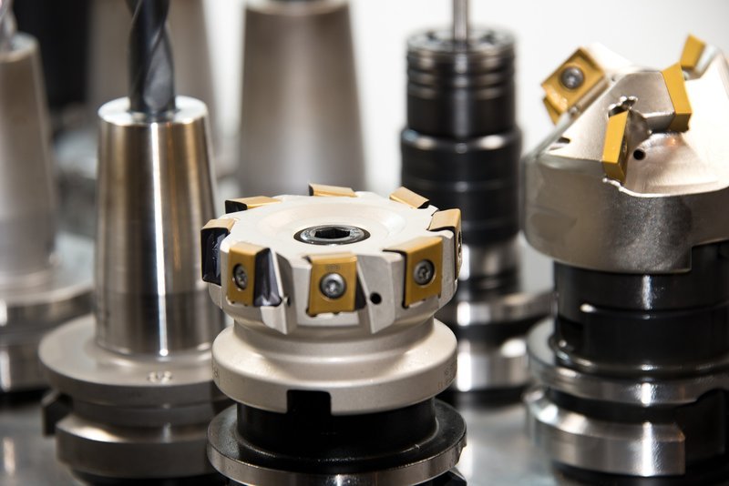
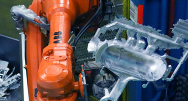
Wafer handling arms and end effectors require exceptional flatness, surface cleanliness, and positional repeatability.
Key Semiconductor Components Requiring Ultra-Precision CNC Machining
Wafer Handling Systems
Wafer handling arms, end effectors, and transfer robots demand ultra-flat surfaces and precise geometry for vacuum-compatible motion. Components are machined from aluminum 6061, titanium, or PEEK, with positional accuracy ≤ 0.005 mm.
Vacuum Chamber Components
Chamber bodies, covers, flanges, and sealing surfaces must maintain airtight sealing under high vacuum. 5-axis CNC creates O-ring grooves, port flanges, and internal channels in a single operation. Helium leak testing ≤ 1×10⁻⁹ mbar·L/s.
Gas Distribution Systems
Showerheads and distribution plates deliver process gases uniformly across wafer surfaces. Hole position accuracy of ±0.02 mm and internal surface finish of Ra ≤ 0.4 μm are typical requirements.
Electrostatic Chuck Components
ESC base plates demand perfect planarity and dielectric separation zones. These components hold wafers during etching or deposition and must maintain temperature uniformity within ±0.5°C.
Quality Assurance and Inspection Standards
- Dimensional Inspection: 100% CMM inspection of critical features, with temperature-controlled metrology labs at ±1°C.
- Surface Roughness Testing: Profilometer or white light interferometry to ensure Ra requirements.
- Cleanliness Verification: Particle counting per SEMI standards with outgassing analysis reports.
- Material Certification: Full traceability from mill to finished component.
- Process Capability: Cpk ≥ 1.67 for critical features across production lots.
2026 Market Data: The global semiconductor equipment market is projected to reach US$165.9 billion in 2026, with front-end wafer processing equipment accounting for over 80% of total sales.
How SOMI Custom Parts Can Help
At SOMI Custom Parts, we combine advanced 5-axis CNC machining capabilities with rigorous quality systems to deliver semiconductor equipment components that meet the industry's most demanding requirements. Our temperature-controlled facility supports tolerances as tight as ±0.003 mm, and we implement strict contamination control protocols including multi-stage ultrasonic cleaning and Class 100 cleanroom packaging.
Our engineering team provides comprehensive Design for Manufacturability (DFM) feedback, helping OEMs optimize part geometry for performance and manufacturability. We work with aluminum alloys, stainless steel, PEEK, ceramics, and titanium. Explore our CNC machining services or contact our team to discuss your project.
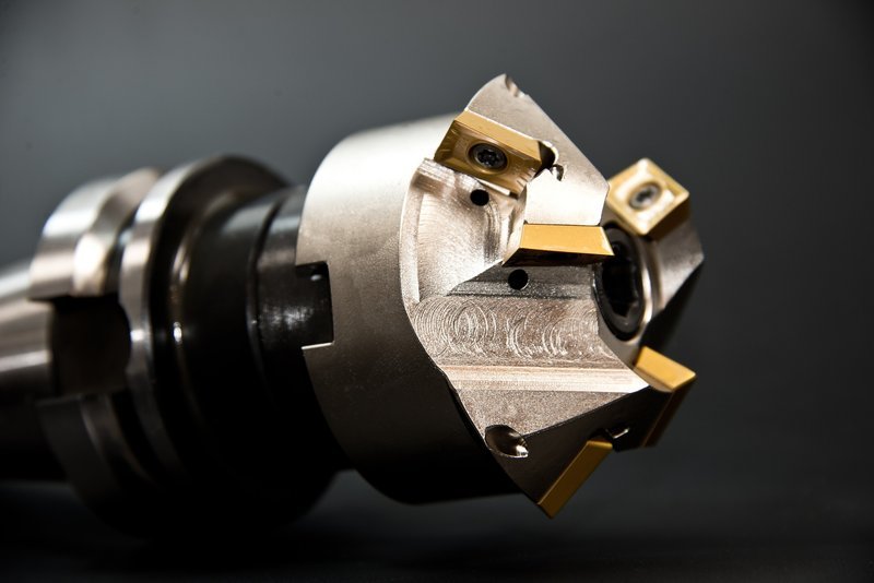
SOMI Custom Parts delivers ultra-precision CNC machining for semiconductor equipment manufacturers worldwide.
Frequently Asked Questions
What tolerances can CNC machining achieve for semiconductor equipment parts?
Standard semiconductor-grade CNC machining achieves tolerances of ±0.005 mm, with ultra-precision capabilities reaching ±0.001 mm (1 micron) for critical features.
What materials are commonly used in semiconductor CNC machining?
Common materials include aluminum alloys (6061-T6, 7075-T6), stainless steel (316L, 304), titanium, engineering plastics (PEEK, Vespel, PTFE), and technical ceramics (alumina, silicon carbide).
How is contamination prevented during semiconductor part manufacturing?
Contamination prevention involves cleanroom-compatible processes, multi-stage ultrasonic cleaning with DI water, vacuum bake-out at 150–200°C, particle counting, and Class 100 cleanroom packaging.
What certifications should a semiconductor CNC machining supplier have?
Key certifications include ISO 9001:2015, ISO 13485, SEMI S2/S8 compliance, and ITAR registration for defense applications. Material traceability and outgassing test reports should be available.
How does semiconductor-grade machining differ from conventional CNC machining?
The key difference is the simultaneous combination of tight tolerances, geometric controls, surface finish, cleanliness, traceability, and repeatability—all required at once.
Conclusion
CNC machining for semiconductor equipment represents the highest tier of precision manufacturing, where micron-level accuracy, contamination control, and material science converge to enable next-generation chip fabrication. With the global semiconductor equipment market projected to reach US$229.5 billion by 2028 per SEMI, demand for ultra-precision CNC-machined components will only intensify.
If you are developing next-generation semiconductor equipment, reach out to SOMI Custom Parts. Our engineering team provides DFM feedback and precision machining solutions for the most demanding semiconductor applications. Explore more industry insights on our blog.